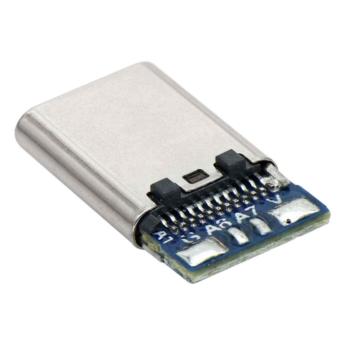
Key elements of solderless press in PCBA connection technology
Solderless press in type PCBA Connection technology, also known as crimping technology, is to insert two or more sides through elastic deformation joints or rigid joints.
The utility model relates to a moderate press in connection composed of a metallized hole of a laminated plate, which forms a close contact point between the joint and the metallized hole, and realizes electrical connection through mechanical connection.
The crimping technology has the advantages of high reliability, safe insertion and easy operation, avoids the problem of excessive heat absorption of the connector during reflow soldering, and will not cause damage or fracture of the plug; At the same time, there is no need for solder and flux, which solves the problems of difficult cleaning of weldments and easy oxidation of welding surface. Therefore, crimping technology is still widely accepted and used

PCBA Key elements of crimping technology:
① Press in the connector; ② Printed board; ③ Crimping process; ④ Crimping tools and equipment.
The press in connector (crimping pin) is divided into rigid pin and flexible pin. The rigid pin will not deform during crimping, and the hole will deform.
The flexible pin will be extruded and deformed during crimping, and the hole will not be deformed.
Copper alloy of appropriate grade shall be used for crimping. Such as copper tin alloy, bronze zinc alloy, brass or beryllium copper alloy.
The selection of materials depends not only on the size and function of parts, but also on good and stable electrical connection requirements.
All materials are related to time, temperature and stress, resulting in stress relaxation.
The material and structure of the joint will not reduce the connecting force, so as to increase the resistance at the joint to an unacceptable level.
whole PCBA Machining process is a complex process that needs detail control. Any quality problem of SMT patch and even PCB optical board may lead to poor products.
Shenglan Technology Co., Ltd_ It focuses on the production of electronic connectors and research and development of precision components. Its products are widely used in consumer electronics, new energy vehicles, USB, 5g and other fields. Its industrial lines cover the Pearl River Delta, Southeast Asia and other regions. It has established long-term strategic cooperation relations with well-known enterprises such as Foxconn, Lixun precision, Huawei, Xiaomi, TCL, Hitachi Group, BYD and Great Wall Motors, with IATF 16949, ISO9001 ISO14001, QC080000 and other system certification and product safety certification, and provide professional connection and manufacturing solutions for the industry http://jctc.com.cn/


